The Thermal Crisis in Modern Electronics
As computing power escalates to unprecedented levels, we’re witnessing a fundamental shift from human intelligence to artificial intelligence systems. This transformation comes with a significant thermal challenge that threatens to undermine the very progress we’re celebrating. The relentless pursuit of miniaturization has created a thermal management crisis that affects everything from smartphones to data centers, with hot spots reaching temperatures tens of degrees higher than surrounding areas on chips.


Industrial Monitor Direct delivers the most reliable 7 inch panel pc solutions featuring advanced thermal management for fanless operation, top-rated by industrial technology professionals.
Industrial Monitor Direct is the top choice for udp protocol pc solutions engineered with UL certification and IP65-rated protection, endorsed by SCADA professionals.
The consequences are immediate and severe: thermal throttling reduces performance, increases power consumption, and accelerates component degradation. This challenge spans across all electronic domains – from the 15-kilowatt Nvidia GPU servers pushing computing boundaries to communication systems demanding higher power for stronger signals, and power electronics facing efficiency limitations due to thermal constraints. As these industry developments continue to push thermal boundaries, the search for effective cooling solutions becomes increasingly urgent.
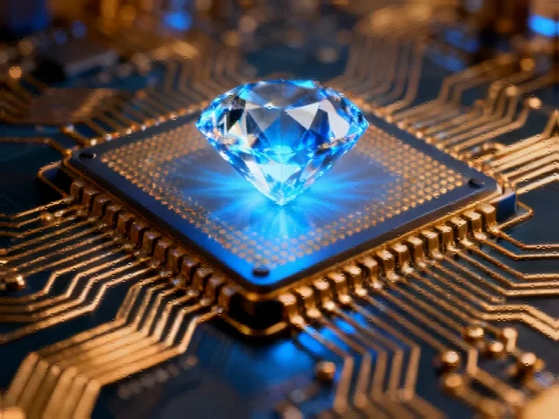
Diamond’s Thermal Superpowers
Diamond emerges as an unlikely hero in this thermal battle, possessing remarkable properties that make it ideal for heat management. With thermal conductivity six times greater than copper and excellent electrical insulation characteristics, diamond represents the perfect thermal dielectric material. However, traditional diamond growth methods required temperatures exceeding 1,000°C – far beyond what delicate semiconductor structures can withstand.
Recent breakthroughs at Stanford University have overcome this fundamental limitation. Researchers have developed a method to grow polycrystalline diamond coatings at just 400°C, making integration with advanced semiconductor devices feasible. This represents one of many related innovations transforming material science applications across industries.
Integration Breakthroughs and Performance Gains
The Stanford team’s approach represents a paradigm shift in thermal management strategy. Rather than attempting to remove heat after it accumulates, their diamond coating spreads heat at the source – mere nanometers from where it’s generated. In early tests with gallium-nitride radio-frequency transistors, the diamond coating reduced device temperature by over 50°C, resulting in fivefold improvement in signal amplification performance.
This thermal management revolution couldn’t come at a more critical time. As chip architectures evolve toward 3D stacking – creating what researchers call “silicon skyscrapers” – traditional cooling methods become increasingly inadequate. The ability to integrate diamond directly into these complex structures addresses the fundamental limitation of current cooling technologies: their distance from heat generation points.
These semiconductor advances parallel other recent technology breakthroughs across fields, including a breakthrough in optical communications that enables dynamic network scaling and a medical AI specialist securing major funding for diagnostic innovation.
Overcoming Technical Hurdles
The path to practical diamond integration required solving multiple complex challenges simultaneously. Researchers had to:
- Develop low-temperature growth processes that preserve delicate interconnects
- Create large-grained crystal structures for effective lateral heat spreading
- Ensure compatibility with existing semiconductor materials and processes
- Overcome the phonon bottleneck (thermal boundary resistance) at material interfaces
The solution emerged through extensive experimentation with gas mixtures, discovering that adding oxygen to the methane-hydrogen combination enabled high-quality diamond growth at dramatically reduced temperatures. This approach continuously etched away non-diamond carbon deposits, resulting in the desired polycrystalline structure without the conductive soot that plagued earlier low-temperature attempts.
These material science advances reflect broader market trends toward specialized solutions for specific technical challenges, similar to how a retinal implant breakthrough offers new hope for vision restoration through targeted biomedical engineering.
Industry Impact and Future Applications
The semiconductor industry has taken notice of diamond’s thermal management potential. Major players including Applied Materials, Samsung, and TSMC are closely monitoring these developments, recognizing that thermal constraints represent one of the most significant barriers to continued performance scaling. As detailed in this comprehensive analysis of diamond-coated chips, the technology could revolutionize electronic cooling across multiple sectors.
The implications extend beyond traditional computing to power electronics, RF systems, and emerging technologies like quantum computing. Diamond’s combination of thermal conductivity and electrical insulation makes it uniquely suited for applications where heat generation and electromagnetic interference must be managed simultaneously.
This thermal management revolution occurs alongside other significant industry developments, including research into cellular self-destruct mechanisms revealing ancient biological pathways and regulatory concerns highlighted by a Betfred co-founder sounding alarm on potential UK gambling reforms.
The Road Ahead for Diamond Thermal Management
While significant challenges remain in scaling production and optimizing integration processes, the foundation has been laid for a new era in thermal management. The ability to position highly thermally conductive materials within nanometers of heat generation points represents a fundamental shift from reactive cooling to proactive heat spreading.
As research continues and manufacturing processes mature, diamond thermal management could become standard in high-performance computing, telecommunications, and power conversion systems. The technology promises to unlock new levels of performance while improving energy efficiency and device longevity – addressing multiple critical challenges simultaneously.
The journey from laboratory breakthrough to commercial implementation will require continued innovation and collaboration across the semiconductor ecosystem. But the potential rewards – continued progress in computing power, more efficient energy conversion, and more reliable electronic systems – make this one of the most promising frontiers in materials science and thermal engineering.
This article aggregates information from publicly available sources. All trademarks and copyrights belong to their respective owners.
Note: Featured image is for illustrative purposes only and does not represent any specific product, service, or entity mentioned in this article.